Sandboxels is a sandbox game where players can create and manipulate elements on a grid, similar to falling sand games. It provides a flexible environment for experimentation with various materials and circuits, allowing players to design and test their own simulations and contraptions. Learn more about Sandboxels.
LogicGates.js is a mod for Sandboxels that adds basic digital logic gates, such as AND, OR, and XOR. This mod builds on the core functionality of Sandboxels by providing essential building blocks for creating simple digital circuits and logical systems.
BetterSettings.js is required for circuitcore, it adds a better settings menu.
CircuitCore.js is an advanced mod that extends the functionality of LogicGates.js by introducing more complex and sophisticated circuits. While LogicGates.js adds fundamental logic gates to Sandboxels, CircuitCore.js builds on these basics to offer advanced components like registers, counters, shift registers, and various arithmetic circuits. This mod enables players to design and construct intricate electronic systems and simulations.
Welcome to the CircuitCore.js documentation. This file provides an overview and basic documentation for each circuit type available in the CircuitCore.js mod. The circuits are categorized by their functionality and color-coded for easy identification. LogicGates.js and betterSettings.js is required for CircuitCore.js. You can also rotate circuits using the up arrow key.
Back to Mods
ROM/RAM
Encoders and De-multiplexers
Decoders and Multiplexers
Program Counter and Shift Registers
Registers
Latches and Flip-Flops
Addition/Subtraction Arithmetic
Complex Circuits
Clocks
Misc and I/O
Displays/Visual Circuits
ROM Circuit
Description: Read-only memory circuit used for storing permanent data. N bit address lines on the left and 4 bit output on the right. Each hex value in ROM is color-coded one of 16 colors.
The circuit is not included in-game yet because I need to add more tools to program the ROM.
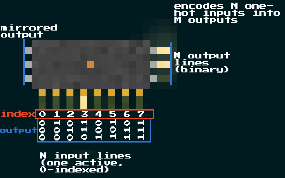
N-to-M Encoder Circuit
Description: Encodes N one-hot input lines on the bottom into M output lines. There are two copies of the output lines, on the left and right. N = 2^M.

1-to-M De-multiplexer Circuit
Description: De-multiplexes 1 input line on the bottom into M output lines on the right based on the N input lines on the left. M = 2^N.

N-to-M Decoder Circuit
Description: Decodes N input lines on the bottom into M one-hot output lines on the left and right (mirrored). M = 2^N.

N-to-M Multiplexer Circuit
Description: Multiplexes N input lines on the left into 1 output line on the right using M input lines on the bottom.

4-bit PISO Shift Register Circuit
Description: A Parallel In Serial Out shift register. Parallel data comes from the top and comes out in serial through the first right output line. Second right output line signifies if the data is currently being transferred, first input line on the left controls when to send start parallel to serial conversion, second input line on the left is clock input.

4-bit SIPO Shift Register Circuit
Description: A Serial In Parallel Out shift register. Serial data comes from the first left input line and is converted to parallel output through the four right output lines. The second left input line is the clock input, and the register shifts data on the rising edge of the clock signal.

4-bit Register Circuit
Description: General-purpose register for storing 4-bit data. Four input bits of input data come from the top. The first right pin is enable, it allows the write enable to work and outputs the stored value in the register. The second right pin is write enable, it allows the input data to get written to the register, it will only work if the first enable pin is also on.

SR Latch Circuit
Description: Set-Reset latch for basic memory storage. Enable the top pin to activate the outputs on the left and right, Enable the bottom pin to disable the outputs on the left and right.

T Flip-Flop Circuit
Description: Toggle flip-flop for binary counting and state storage. When the top input has a rising edge, the state of the left and right pins toggles.

D Latch Circuit
Description: A D latch circuit for data storage. The data input is on the top, and the enable input is on the right. When the enable input is active, the data input is stored and outputted on the left and bottom.

D Flip-Flop Circuit
Description: A D flip-flop circuit for edge-triggered data storage. The data input is on the top, and the control input is on the right. The data is transferred to the output on the left and bottom on the rising edge of the control input.

4-bit D Latch Circuit
Description: A 4-bit D latch for storing 4-bit data. The data inputs are on the top (D0-D3) and the control input is on the right. When the control input is active, the data inputs are stored and outputted on the bottom (Q0-Q3).

4-bit D Flip-Flop Circuit
Description: A 4-bit D flip-flop for edge-triggered data storage. The data inputs are on the top (D0-D3) and the control input is on the right. The data is transferred to the output on the bottom (Q0-Q3) on the rising edge of the control input.

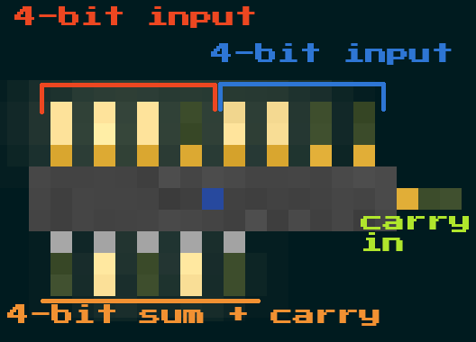
4-bit Adder Circuit
Description: Performs binary addition on two 4-bit numbers. The first 4-bit number inputs are on the left (A0-A3), the second 4-bit number inputs are on the right (B0-B3), and the carry-in input is on the far right. The sum outputs are on the bottom (S0-S3).

Clock Circuit
Description: Generates a regular clock signal for use in synchronous circuits. Includes adjustable frequency settings.
Custom I/O Circuit
Description: This circuit allows custom input and output configurations for various digital applications. It includes general-purpose pins for user-defined functionality, enabling flexible circuit designs.
Logic Probe
Description: A simple circuit used for debugging and testing digital logic. It can detect and display the logic level (high or low) of a circuit at a specific point.
Bus Splitter
Description: A circuit that splits a single bus into multiple outputs, allowing for easy routing and management of data lines in complex circuits.
Binary to BCD Converter
Description: Converts binary numbers to Binary-Coded Decimal (BCD) format, facilitating easy integration with display circuits like 7-segment displays.

7-segment Display Circuit
Description: Displays binary or decimal values using a 7-segment display. Includes connections for data input and segment control.

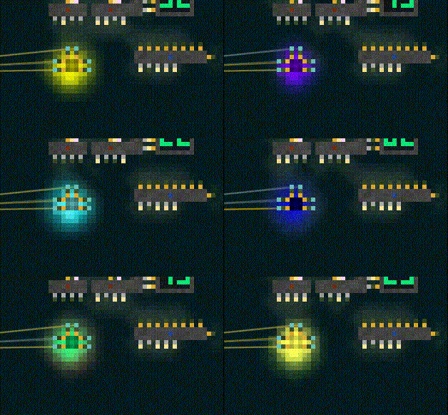
RGB LED Circuit
Description: A customizable RGB LED circuit that can display a wide range of colors based on the digital inputs it receives. The circuit accepts 6 input lines, 2 for each of the Red, Green, and Blue components, allowing for precise color control. The output color is displayed across a 3x3 grid around the pixel, creating a smooth lighting effect.
